Powered USB hubs would reduce the number of power sources required, so I did just that. Lots of cables would get in the way so I designed a custom "backplane" USB hub with male mini-B ports which could plug directly into small prototyping boards. (As a side note, the connectors for this board were nearly impossible to find. There are very few uses for a male mini-B connector that mounts to a PCB rather than being attached to a cable so nobody makes them!)
 |
| USB backplane hub |
The obvious first idea was an ATX supply. My calculations of peak power for the apparatus (including room for growth) were fairly high, though, and most ATX supplies put the bulk of their output on the 12V rail and have fairly limited (well under 100W) 5V capacity.
The next thing I considered was an off-the-shelf 5V supply. This looked like a nice idea, but (as with an ATX supply) the high output current capability would represent a fire hazard if something shorted. I would obviously need overcurrent protection.
Thinking a bit more, I realized that fusing was probably not the best option. Fuses need to be replaced once blown and in a lab environment overcurrent events happen fairly often. Classical current limiting techniques would be problematic as well since many of my boards have switching power supplies. Since a switcher is a nonlinear load, reducing the input voltage doesn't actually reduce the current. Instead, load current actually increases to maintain the output voltage, which can lead to runaway failure conditions. The safer way to handle overcurrent on a switcher is to shut it down entirely.
I also wanted the ability to power cycle boards on command to reset a stuck board or test power-up behavior. While jiggling cables may work in a hands-on lab environment, it isn't a viable option in the remote-controlled "embedded cloud" platform I'm trying to build.
This would obviously require some intelligence on the part of the power management system. The natural solution was a managed power distribution unit (PDU) of the sort commonly used in datacenters for feeding power to racks of servers. Managed PDUs often include current metering as well, which could be very useful to me when trying to minimize power consumption in a design.
There's just one problem: As far as I can tell, nobody makes managed PDUs for 5V loads. The only ones I saw were for 12/24/48V supplies and massively overpriced: this 8-channel 12V unit costs a whopping $1,757.
What to do? Build one myself, of course!
The first step was to come up with the requirements:
- Remote control via SNMP
- Ten DC outputs fed by external supply
- 4A max load for any single channel, 20A max for entire board
- Independent overcurrent shutdown for each channel with adjustable threshold
- Inrush timers for overcurrent shutdown to prevent false positives during powerup
- Remote switching
- Current metering
- Thermal shutdown
- Under/overvoltage shutdown
- Input reverse voltage protection
- Able to operate at 5V or 12V (jumper selected)
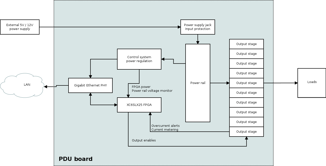 |
| PDU block diagram |
The output stage is key to the entire circuit so it was very important that it be designed correctly. I put quite a bit of effort into component selection here... perhaps a bit too much, as I missed a few bugs elsewhere on the board! More on that later.
 |
| Output stage |
The fuse is provided purely as a second line of defense in the event that the soft overcurrent protection fails. As a firmware/HDL developer I know all too well what bugs are capable of, so I like to include passive safeguards whenever reasonably possible. Assuming that my code works correctly, this fuse should never blow even if the output of the PDU was connected to a dead short. (This of course requires that my protection mechanism trip faster than the fuse. Given the 1ms response time of typical fuses to small overcurrents, this isn't a very difficult task.)
Power switching is done by a high-side P-channel MOSFET connected to VOUT (the main high-current power rail). The logic-level input from the control subsystem is shifted up to VOUT level by an N-channel MOSFET. A pullup and pulldown resistor ensure that the output is kept safely in the "off" state when the system is booting.
 |
| Current monitoring |
A module in the FPGA controls the output enables based on the overcurrent flags and internal state. When an output is first turned on the overcurrent flag is ignored for a programmable delay (usually a few ms) in order to avoid false triggering from inrush spikes. After this period, if the overcurrent flag is ever asserted the channel is turned off and placed in the "error-disable" state. In order to clear an error condition the channel must be manually cycled, much like a conventional circuit breaker.
Here's a view of the finished first-run prototype. As you can see the first layout revision had a few bugs ;) The dead-bugged oscillator turned out to not be necessary but it would have been more work to remove it so I'm keeping it until I do a respin with all of these fixes incorporated.
 |
| PDU board on my desk |
GRAFTON's programming model is largely event-driven, in a model that will be somewhat familiar to anyone who has done raw Windows API programming. The CPU sleeps until an RPC interrupt packet shows up, then it is processed and it goes back to sleep. Unlike classical interrupt handling, user code running on GRAFTON cannot be pre-empted by an interrupt; it just sits in the queue until retrieved.
int main()
{
	//Do one-time setup
	Initialize();

	//Main message loop
	RPCMessage_t rmsg;
	while(1)
	{
		GetRPCInterrupt(&rmsg);
		ProcessInterrupt(&rmsg);
	}

	return 0;
}
RPCFunctionCall(), a simple C wrapper around the low-level SendRPCMessage and RecvRPCMessage() functions, abstracts the RPC network with a blocking C function call semantics. Any messages other than return values of the pending call are queued for future processing.
In the example below, I'm initializing the SPI modules for the A/D converters with a clock divisor computed on the fly from the system clock rate.
void ADCInitialize()
{
	//SPI clock = 250 KHz
	RPCMessage_t rmsg;
	RPCFunctionCall(g_sysinfoAddr, SYSINFO_GET_CYCFREQ, 0, 250 * 1000, 0, &rmsg);
	int spiclk = rmsg.data[1];
	for(unsigned int i=0; i<3; i++)
		RPCFunctionCall(g_periphAddr, PERIPH_SPI_SET_CLKDIV, spiclk, i, 0, &rmsg);
}
The firmware is about 4300 lines of C in total, including comments but not the 1165 lines of C and assembly in my C runtime library shared by all GRAFTON designs. It implements IPv4, UDP, DHCP, ARP, ICMP echo, and SNMPv2c. SNMPv3 security and IPv6 are planned but are on hold until I move firmware out of block RAM and into flash so I have some space to work in. Other than that, it's essentially feature-complete and I've been using the PDU in my lab for a while while working on my flash controller and some support stuff.
The PC-side UI, intended to control several PDUs, is written in C++ using gtkmm and communicates with the board over SNMP. One tab (not shown) contains summary information with one graph trace per PDU.
 |
| PDU control panel |
 |
| Munin logs of PDU |
It needs a little bit more work to be fully production-ready but is already saving me time around the lab.
 |
| My desk with the PDU installed |
Very impressive stuff! Look forward to hearing more about the processor design.
ReplyDelete